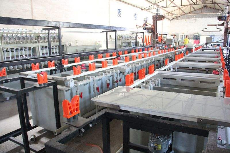
Eight kinds of PCB surface treatment process
- 8月 23, 2017
- 11:35 下午
With the continuous improvement of living environment, the environmental problems involved in PCB production are especially prominent.The topic of lead and bromine is the most popular, and the development of PCB will be affected in many ways by lead-free and halogen-free.
Although for now, the change of the PCB surface treatment technology and is not very big, still more distant things like, but should notice: long-term slow change will result in great changes.In the case of increasing environmental demand, the surface treatment technology of PCB will definitely change dramatically in the future.
The most basic purpose of surface treatment is to ensure good weldability or electrical performance.Since the natural copper tends to exist in the air in the form of oxides, it is unlikely that the copper will be kept for a long time. Therefore, other treatment of copper will be required.Although most copper oxides can be removed in the subsequent assembly, the strong flux is not easy to remove, so the industry generally does not use strong flux.
There are many PCB surface treatment processes, which are commonly used in the five processes of hot-air leveling, organic coating, electroless nickel/leaching, dip silver and tin.
1. Hot air leveling (spray tin)
Hot air leveling and hot air solder leveling (commonly known as spray tin), it is coated on the PCB surface heating molten tin solder (lead) and total compressed air (blow) flat craft, make its form a layer of copper oxidation resistance, and can provide good weldability of the coating layer.The solder and copper are formed in the junction of copper and Sikkim compound.The PCB has to be immersed in molten solder at normal times.The windknife blows the liquid solder before the solder solidifies;The windknife can minimize the bending of the solder on the copper surface and prevent the welding bridge.
2. Organic weldable protective agent (OSP)
OSP is a process that conforms to RoHS directive requirements for PCB copper foil surface treatment.OSP is an abbreviation of Organic Solderability preservative. It is also known as Preflux, and also known as Preflux.In a nutshell, the OSP is on clean, bare copper surfaces and chemically grows a layer of organic membranes.
This film has anti-oxidation, heat resistance and moisture resistance to protect the copper surface from rust (oxidation or vulcanization etc.) in normal environment.But in the subsequent welding heat, the protective film and must be quickly removed by flux easily, so just can make clean copper surface of the show is in a very short period of time with molten solder immediately become a solid solder joints.
3. Full plate nickel plating
Nickel-plated nickel plating is a layer of nickel plating on the surface of the PCB, which is then plated with a layer of gold. The nickel plating is mainly used to prevent the spread of gold and copper.Now there are two types of electroplating nickel gold: soft gold plating (gold, gold surface looks not bright) and hard gold plating (surface is smooth and hard, wear-resisting, contain other elements such as cobalt, gold looks more light).Soft gold is mainly used for chip packaging and gold wire.Hard gold is mainly used in the electrical interconnection of non – weld.
4, zedoary
The sinking gold is covered in a thick, electrical, good nickel-gold alloy on the copper surface, which can protect the PCB for a long time.It also has the tolerance for the environment that other surface treatment processes do not have.It also prevents the copper from dissolving, which would be good for lead-free assembly.
5, sink a tin
As the solder is currently based on tin, the tin can match any type of solder.Tin process between flat copper tin compounds can be formed, this feature makes heavy tin has like hot air leveling of good weldability and no hot air leveling flatness of headache problem;The tin plate cannot be stored for too long and must be assembled according to the sequence of tin.
6, heavy silver
Silver settling process is between organic coating and electroless nickel/sinking gold. The process is simple and quick.Even when exposed to heat, humidity and pollution, the silver can still be weldable, but it will lose its luster.The silver plating does not have the good physical strength of the chemical nickel-plated/sinking gold because there is no nickel under the silver layer.
7. Chemical nickel palladium
The chemical nickel palladium is a layer of palladium between nickel and gold. Palladium can prevent the corrosion phenomenon caused by substitution reaction, and make full preparation for the sinking.Gold closely covers the palladium and provides a good interface.
8. Electroplating hard gold
In order to improve the wear-resisting property of the product, increase the number of inserts and the plating hard gold.
As users demand more and more high, environment is becoming more and more strict, surface treatment technology is more and more, whether to choose the sort of promising, stronger commonality of surface treatment technology, it seems like a bit dazzling, uncertain.It is impossible to predict the future direction of PCB surface treatment technology.Either way, meeting user requirements and protecting the environment must be done first!


